- 您现在的位置:买卖IC网 > Sheet目录338 > LT3956EUHE#PBF (Linear Technology)IC LED DVR BUCK BOOST 36-VQFN
LT3956
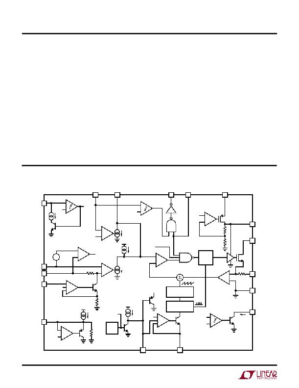
PIN FUNCTIONS
V REF : Voltage Reference Output Pin (typically 2V). This
pin drives a resistor divider for the CTRL pin, either for
analog dimming or for temperature limit/compensation
of LED load. Can supply up to 100μA.
PWM: A signal low turns off switcher, idles oscillator and
disconnects V C pin from all internal loads. PWMOUT pin
follows PWM pin. PWM has an internal pull-down resistor.
If not used, connect to INTV CC .
VMODE : An open-collector pull-down on VMODE asserts
if the FB input is greater than the FB regulation threshold
minus 50mV (typical). To function, the pin requires an
external pull-up resistor. When the PWM input is low
and the DC/DC converter is idle, the VMODE condition is
latched to the last valid state when the PWM input was
BLOCK DIAGRAM
high. When PWM input goes high again, the VMODE pin
will be updated. This pin may be used to report an open
LED fault. Use a pull-up current less than 1mA.
SS: Soft-Start Pin. This pin modulates oscillator fre-
quency and compensation pin voltage (V C ) clamp. The
soft-start interval is set with an external capacitor. The
pin has a 10μA (typical) pull-up current source to an
internal 2.5V rail. The soft-start pin is reset to GND by
an undervoltage condition (detected by EN/UVLO pin)
or thermal limit.
RT: Switching Frequency Adjustment Pin. Set the fre-
quency using a resistor to GND (for resistor values, see
the Typical Performance curve or Table 1). Do not leave
the RT pin open.
EN/UVLO
A6
FB
VC
PWMOUT
PWM
V IN
1.22V
2.1μA
SHDN
1.31V
OVFB
COMPARATOR
1.25V
LDO
A8
7.15V
INTV CC
+
–
1.25V
A5
g m
10μA AT
FB = 1.25V
SW
+
+
–
–
+
–
+
–
–
+
–
ISN
ISP
SHORT-CIRCUIT
DETECT
A10
350mV
CTRL
CTRL BUFFER
1.1V + A3
5k
SCILMB
g m
EAMP
A1
Q2
SCILMB
10μA
10μA AT
A1 + = A1 –
VC
SSCLAMP
+
A2
PWM
COMPARATOR
RAMP
GENERATOR
R
S
Q
DRIVER
I SENSE
A4
PGND
GND
+
V REF
2V
A7
20k
140μA
170k
FAULT
LOGIC
TSD
165°C
10μA
1.25V
+
–
100kHz TO 1MHz
OSCILLATOR
FREQ
PROG
1.2V
FB
VMODE
1mA (MAX)
SS
RT
3956f
发布紧急采购,3分钟左右您将得到回复。
相关PDF资料
LTC3201EMS#TRPBF
IC LED DRVR WHITE BCKLGT 10-MSOP
LTC3202EDD#PBF
IC LED DRIVR WHITE BCKLGT 10-DFN
LTC3205EUF#TRPBF
IC LED DRVR WT/RGB BCKLGT 24-QFN
LTC3206EUF#TRPBF
IC LED DRVR WT/RGB BCKLGT 24-QFN
LTC3207EUF-1#TRPBF
IC LED DRIVR QVGA DISPLAY 24-QFN
LTC3208EUH#TRPBF
IC LED DRIVR QVGA DISPLAY 32-QFN
LTC3209EUF-2#TRPBF
IC LED DRIVR QVGA DISPLAY 20-QFN
LTC3210EPD-1#TRPBF
IC LED DRVR WHITE BCKLT 16-UTQFN
相关代理商/技术参数
LT3956EUHE#PBF
制造商:Linear Technology 功能描述:IC LED DRIVER BUCK-BOOST/FLYBACK QFN36
LT3956EUHE#TRPBF
功能描述:IC LED DVR BUCK BOOST 36-VQFN RoHS:是 类别:集成电路 (IC) >> PMIC - LED 驱动器 系列:- 标准包装:6,000 系列:- 恒定电流:- 恒定电压:- 拓扑:开路漏极,PWM 输出数:4 内部驱动器:是 类型 - 主要:LED 闪烁器 类型 - 次要:- 频率:400kHz 电源电压:2.3 V ~ 5.5 V 输出电压:- 安装类型:表面贴装 封装/外壳:8-VFDFN 裸露焊盘 供应商设备封装:8-HVSON 包装:带卷 (TR) 工作温度:-40°C ~ 85°C 其它名称:935286881118PCA9553TK/02-TPCA9553TK/02-T-ND
LT3956EUHEPBF
制造商:Linear Technology 功能描述:80V Constant-Current/Voltage Conv. QFN36
LT3956EUHE-PBF
制造商:LINER 制造商全称:Linear Technology 功能描述:80VIN, 80VOUT Constant-Current, Constant-Voltage Converter
LT3956EUHE-TRPBF
制造商:LINER 制造商全称:Linear Technology 功能描述:80VIN, 80VOUT Constant-Current, Constant-Voltage Converter
LT3956IUHE#PBF
功能描述:IC LED DVR BUCK BOOST 36-VQFN RoHS:是 类别:集成电路 (IC) >> PMIC - LED 驱动器 系列:- 标准包装:6,000 系列:- 恒定电流:- 恒定电压:- 拓扑:开路漏极,PWM 输出数:4 内部驱动器:是 类型 - 主要:LED 闪烁器 类型 - 次要:- 频率:400kHz 电源电压:2.3 V ~ 5.5 V 输出电压:- 安装类型:表面贴装 封装/外壳:8-VFDFN 裸露焊盘 供应商设备封装:8-HVSON 包装:带卷 (TR) 工作温度:-40°C ~ 85°C 其它名称:935286881118PCA9553TK/02-TPCA9553TK/02-T-ND
LT3956IUHE#TRPBF
功能描述:IC LED DVR BUCK BOOST 36-VQFN RoHS:是 类别:集成电路 (IC) >> PMIC - LED 驱动器 系列:- 标准包装:6,000 系列:- 恒定电流:- 恒定电压:- 拓扑:开路漏极,PWM 输出数:4 内部驱动器:是 类型 - 主要:LED 闪烁器 类型 - 次要:- 频率:400kHz 电源电压:2.3 V ~ 5.5 V 输出电压:- 安装类型:表面贴装 封装/外壳:8-VFDFN 裸露焊盘 供应商设备封装:8-HVSON 包装:带卷 (TR) 工作温度:-40°C ~ 85°C 其它名称:935286881118PCA9553TK/02-TPCA9553TK/02-T-ND
LT3956IUHE-PBF
制造商:LINER 制造商全称:Linear Technology 功能描述:80VIN, 80VOUT Constant-Current, Constant-Voltage Converter
